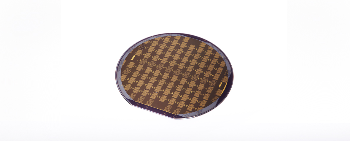
2-dimensional (2D) materials are crystalline materials with a single layer of atoms and ultrathin nanomaterial with a high degree of anisotropy. There are only van der Waals interactions between the layers, and no surface states or dangling bonds. Representative 2D materials include metallic graphene, semiconductor Transition Metal Dichalcogenide (TMD) and Black Phosporouse (BP), and insulating hexagonal-Born nitride (h-BN).

2D materials have been considered as one of the key materials for future electronic devices in the sense that representatives of them have following properties. First, graphene has many extraordinary properties in carrier mobility, flexibility, chemical inertness, and thermal conductivity. Thus, it has attracted attentions in various applications, such as high performance transistor, flexible electronics, transparent electrode, supercapacitor and heat sink. Second, TMDs with various band gap (0.3~4.0eV) can absorb light of a wide spectrum from the visible region to the IR region. Therefore, those materials have been considered in optoelectronic applications, such as IR photodetector, photoswitch, and light emitting diode (LED). In addition, thanks to their band gap, TMD and BP are considered as potential materials for logic devices.

2D materials research has been undertaking in two directions. One is to improve the performance of conventional silicon devices. The size of transistor has been constantly reduced while improving performance as well as power consumption. Graphene and h-BN have been introduced as components of present silicon devices to control the interfaces, to improve fabrication processes, and the performance with resistance reduction. The other direction is developing a new concept device research beyond silicon devices such as low-power transistor at sub 5nm and optoelectronic transistor in IR regime. Sticking by those directions in our research, we explore from large scale 2D materials development to device integration.