We have conducted fundamental research on machine learning algorithms, computer vision, and language understanding, and applied them to build industrial AI solutions in the fields of semiconductor manufacturing, materials discovery, and autonomous machines.
We are transforming semiconductor R&D and manufacturing processes using cutting-edge AI technologies like deep learning and generative AI. This AI-based transformation creates fundamental changes across various areas, from chip design to process development, yield optimization, metrology and inspection, fab monitoring and automation, customer and business environment analysis, and decision-making.
-
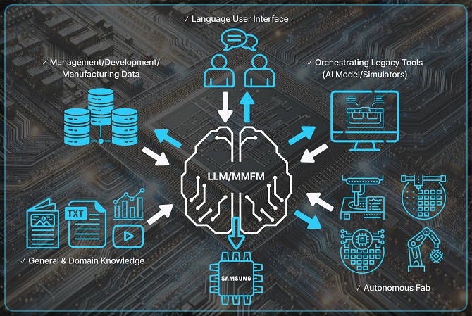
Large language models (LLMs) are key inference engines that can be used in all semiconductor manufacturing and development fields by learning semiconductor knowledge and reasoning capabilities from various types of text data, such as semiconductor reports, papers, patents, technical reports, and general text data, and use it to assist semiconductor engineers and automate the entire manufacturing process.
-
A multimodal foundation model (MMFM) is an advanced type of artificial intelligence that can process and integrate multiple types of data such as documents, images, text, charts, tables, and sensor data.
These models are useful for semiconductor manufacturing and development because they can assist with tasks such as defect reasoning, quality control, design optimization, and data analysis. -
AI innovation is required to support critical decision making in sales and customer responses. AI can analyze customer quality data to prioritize response strategies and efficiently handle tasks related to customer issues. It can also analyze information about the semiconductor industry to identify demand patterns and establish marketing strategies by predicting future purchase demands.
-
Semiconductor design is a complex and time-consuming task that requires significant investments, and AI technology can maximize its efficiency. AI can quickly analyze large volumes of design data, optimize and solve complex problems that arise during the design process, and perform such tasks as reducing defects through problem analysis on a scale beyond human limitations. This can significantly improve productivity in the fast-paced design industry and enhance product quality.
-
We maximize the efficiency of semiconductor R&D by applying AI technology. By identifying and optimizing potential problems throughout the process, we can reduce the lead time for process development, and by developing AI models that reflect the physical and chemical knowledge of the process, we can improve the final product‘s performance, even with small sets of sample data.
-
To measure and inspect increasingly complex and smaller semiconductor structures, AI models utilize various inputs, such as scanning electron microscopy, optical microscopy, atomic force microscopy, X-ray, ellipsometry, and time-series data, to predict 3D structures and detect defects. Ultimately, AI technology is employed to predict structures and defects using data from throughout the semiconductor manufacturing process, control the factors that cause defects, and improve the process.
-
We apply deep learning to semiconductor manufacturing for automated detection of potential faults, process optimization, and yield prediction & analysis to maximize manufacturing performance. Research topics in semiconductor manufacturing include machine learning, deep learning, anomaly detection, explainable AI, Bayesian optimization, large language Models, and data engineering and science.
-
Data management is one of the toughest hurdles to surmount in bringing advanced AI algorithms to the industry. Working closely with experts in the field, we are actively developing technologies to enable AI to handle every aspect of data processing from collection and cleansing to processing and usage by itself.
-
Entering the foundation model era, we are making notable changes in the operating functions that are essential for efficiently managing data and aligning, deploying, optimizing, and monitoring large models within the framework of AI systems. In particular, we are working on building a data pipeline and SW platform (FMOps) that can efficiently develop and utilize semiconductor-specific models using various large unstructured data.
Our materials discovery AI research aims to develop technologies that can assist in developing materials across various industrial sectors by leveraging AI technologies. These technologies may include methods to sense new technologies and explore and optimize the molecular structure and synthesis recipe of materials with desired properties. These technologies can play a major role in many areas, not only by supporting researchers to efficiently complete various tasks required for material discovery but also by helping them make decisions to effectively explore the search space for complex and wide-ranging optimization problems in the field of material discovery.
We are advancing AI technologies through collaboration with high-priority material discovery projects within the Samsung Group to meet domain-specific requirements and directly achieve our materials development goals.

Advancements in display technology have necessitated research and development on cutting-edge materials like OLED and Quantum Dots (QDs). These materials play a vital role in maximizing display performance and enhancing user experience. The application of Artificial Intelligence (AI) in this field has resulted in revolutionary changes, where AI serves as a critical tool for analyzing complex data and predicting the physical and chemical properties of materials. AI contributes to the exploration of new material combinations, optimizing performance and increasing the efficiency of production processes.
The role of AI in the development of OLED and QD materials is becoming increasingly significant. In addition, AI leverages large datasets to learn the complex relationships between the characteristics and performances of materials, thereby supporting material researchers in designing and optimizing target materials more quickly and accurately. This will accelerate the development cycle and open up possibilities for the rapid introduction of innovative display materials to the market. Such applications of AI mark a pivotal turning point in the future of materials discovery in the display domain.
The semiconductor industry requires continuous technological innovation, and the development of material/process technologies is a key element of this innovation. With the recent combination of AI technology with chemical and materials science, the use of AI technology is also playing an important role in research and development processes to explore materials and improve process/analysis technologies.
Based on advanced data analysis, an AI model for predicting experimental results and proposing experimental conditions affords us the potential to efficiently reduce the cost of research and development. In particular, the AI model can quickly derive optimal material combinations and process methods by considering numerous chemical and physical properties, which can accelerate the development of high-performance low-power semiconductors. In addition, it improves the efficiency of the research process through risk management in experiments and allows material development researchers to focus on advanced R&D processes. As such, the integration of AI technology is becoming an important driving force for innovatively changing the future of semiconductor material discovery.
We are focusing on developing AI technology to develop various materials and process optimizations to enhance the competitiveness of our semiconductor technology and implement next-generation semiconductors.
We will secure Samsung’s future technological competitiveness by realizing autonomous machine technology that perceives, judges, and acts like humans through embodied AI technology, which represents the next state of AI innovation, following generative AI and large language models.
We are pioneering the development of embodied AI technology, a groundbreaking innovation that not only operates autonomously with its own physical form but also learns and adapts through dynamic interaction with its environment. This technology harnesses humanlike cognitive abilities to make independent decisions. The core of embodied AI consists of situation awareness intelligence, which comprehends the causality and dynamics of the physical world by utilizing data from diverse modalities at a human-like level, and motion intelligence, which is capable of executing precise machine control while adapting seamlessly to ever-changing environments.
We are developing an embodied AI technology that perceives and makes decisions similar to those of humans. Unlike traditional robot technologies, which focus on designing robot behaviors by recognizing the types of objects and spatial information in the environment, our embodied AI technology predicts the actions that robots should perform based on an understanding of physical phenomena, object properties, and human-like reasoning. This will enable us to solve complex and diverse problems that are difficult for humans to design, and to implement autonomous decision-making AI technology.
We are currently developing AI technologies related to the motion and mobility of future robots. Using embodied AI technology, we are creating robot-specific motion AI models that perform complex and diverse tasks in real-world scenarios with greater speed and efficiency.
These models foster intelligent, adaptive, and interactive capabilities, ensuring that our autonomous machines possess cutting-edge motion intelligence. Through these advancements, we will secure the core technologies that are essential for the future of autonomous robotics.