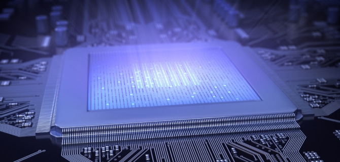
Si-Photonics is a technology that integrates multiple photonic functions onto a silicon-based chip, manipulating light for various applications, including optical communication and processing.
Meta-Photonics explores innovative photonic devices made up of artificial nanostructures that enable new optical behaviors by customizing the optical response of each nanostructure.

Silicon photonics refers to the technology that utilizes silicon as a platform for the generation, manipulation, and detection of light (photons). It aims to integrate photonic functions (like light sources, modulators, detectors, and waveguides) with electronic circuits on a single silicon substrate. Optical interconnects specifically utilize silicon photonics to transmit data using light instead of traditional electrical signals over copper wires. Silicon photonics for optical interconnects represents a significant advancement in data transmission technology, offering advantages in speed, bandwidth, power efficiency, and integration capabilities over traditional electrical interconnects.

The trend of Meta-Photonics technology is evolving from basic research on principles to various advanced studies and new applications. Whereas the design technology has focused simple look-up table methods so far, which facilitate the changes of the phase and amplitude under altering one to three structures parameters at most in a unit cell, it has now advanced to designing high-complexity super cells for multifunctional capabilities. Additionally, with the introduction of inverse design technologies, high performance is being achieved in smaller form factors using new, non-intuitive structures. In terms of fabrication innovations, large-area and cost-effective manufacturing technologies are developing for various practical products. For example, high volume manufacturing technologies such as large-area photolithography, nanoimprint, and roll-to-roll printing are being developed, and another techniques like coating high-refractive-index materials on highly processable low-refractive-index substances are emerging. As design and processing technologies advance, Meta-Photonics is gradually being adopted in various consumer electronics. Infrared machine vision technologies such as liquid crystal-based beam steering and narrow-band dot pattern projectors have been introduced, and it is expected that products for the human vision spectrum in the visible range will appear soon. Furthermore, this technology is expanding into areas such as optical computing for edge detection and quantum metasurfaces.
Silicon photonics is a rapidly evolving field with several key technical trends emerging:
Integration with Electronics: There‘s a growing trend towards integrating photonics with existing silicon electronics. This includes developing methods to fabricate photonic components alongside electronic circuits on silicon chips, enabling efficient data transfer between electronic and photonic domains. Advanced Modulation Techniques: Researchers are exploring advanced modulation techniques such as high-speed modulation and efficient modulation formats (e.g., PAM4) to increase data transmission rates and improve energy efficiency. Miniaturization and Scalability: Efforts are focused on miniaturizing photonic components and making them scalable for mass production. This includes developing techniques for on-chip integration of lasers, modulators, detectors, and passive components. Low Loss Waveguides: Improving the performance of waveguides to minimize optical losses is critical. Researchers are exploring new materials and geometries to achieve lower propagation losses and improve overall efficiency. Wavelength Division Multiplexing (WDM): Implementing WDM techniques in silicon photonics allows multiple wavelengths of light to be transmitted simultaneously through a single optical fiber, increasing data transmission capacity. Application in Data Centers and Telecommunications: Silicon photonics is gaining traction in data centers and telecommunications for high-speed data transmission and energy-efficient communication links over long distances. Hybrid Integration: Combining silicon photonics with other materials such as III-V semiconductors (e.g., indium phosphide) to leverage their superior optical properties for specific applications where silicon has limitations. Photonic Integrated Circuits (PICs): PICs are being developed with increasing complexity, integrating multiple photonic components on a single chip to perform complex functions such as wavelength switching, routing, and signal processing. These trends indicate a vibrant research and development landscape aimed at overcoming current limitations and expanding the practical applications of silicon photonics in various industries.
Light is an electromagnetic wave that arises from the mutual interaction of time-varying electric and magnetic fields. The properties of such wave depend on the type and structure of the medium through which this wave passes. Meta-Photonics represents the study of new optical behaviors beyond conventional optical properties by developing a new space, constructed with various artificial nanostructures.
"Meta," from Greek, means "beyond" and in the context of Meta-Photonics refers to artificial properties that do not exist naturally. These artificial structures can generate unusual but useful phenomena, unanticipated from naturally observed materials. Meta-Photonics is capable of controlling various optical properties such as the amplitude, phase, polarization as well as the wavelength in a sub-wavelength scale. Thanks to this ability, various fields, including sensors, displays, communication, energy, and biotechnology apply the Meta-Photonics usefully.
Recent technology trends include complicated field generation; it has become possible to generate various images depending on the observation angle or the polarization of incident light. These breakthroughs allow complex hologram images for anti-counterfeiting. Ultrathin and planar form factor of the metasurfaces for imaging, i.e., metalens, have attracted significant interest, because this may replace thick and bulky lens systems in cameras and microscopes. The main hurdle is the dispersive property of the material and the resultant limited bandwidth. Recent studies have shown that this can be circumvented by making use of higher-degree-of-freedom super cell or multi-layer metasurfaces, enabling achromatic and broadband metalens. Intriguingly, contrarian moves are emerging as well; people have started to exploit such dispersive property rather than to overcome. The wavelength-dependent response of the metasurface can be utilized to implement ultra-compact spectrometers and hyperspectral imaging devices.
Meanwhile, there has been considerable and on-going effort to dynamically modulate the response of the metasurfaces. This branch is known as the active (reconfigurable) metasurface. Ultrafast and wide-angle wavefront shaping/representation will enable numerous game-changing devices such as holographic displays, beam steering for light detection and ranging (LiDAR), and free-space optical communications.
SAIT develops next generation devices based on Si-Photonics and Meta-Photonics technologies to deliver future UX applications and innovative technologies to overcome industrial limitations in semiconductor processes.
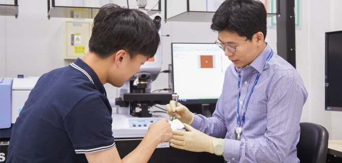
We conduct research on on-chip optical links based on Si-Photonics integrated circuits, which bridge multiple semiconductor devices with dramatically enhanced communication speed. In addition, we develop Meta-Photonics optical structures that enable efficient color splitting for high-sensitive image sensors. Our research area also covers ultra-small and high-resolution LED displays based on III-V semiconductors and optical inspection techniques to improve the performance and process integration of semiconductor devices.
To bring future technologies that enrich our lives, we will cultivate optical technologies that lead innovation in semiconductor devices as well as convey new UX experiences.